
EBSD Explained
Techniques
Applications
Hints and Tips
Technology
OXFORD INSTRUMENTS EBSD PRODUCTS
CMOS Detector RangeAZtecHKL Acquisition SoftwareAZtecCrystal Processing Software
Page 3 of 4
We have already shown that the microstructure is important because it determines many of the physical properties of materials. For example, grain size can influence tensile strength and the properties of grain boundaries can determine the way in which materials fracture. Optical microscopy and scanning electron microscopy are both extensively used to examine microstructures: polishing and chemical etching can reveal the positions of grains and grain boundaries, but these techniques may not reveal all of the grains and provide little quantitative information about either the grains or the boundaries. This is where Electron Backscatter Diffraction (EBSD) comes in – by measuring crystal orientations it can show unambiguously the position and can determine the nature of all grains and grain boundaries.
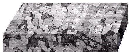
Microstructure revealed on the surface of a sample by chemical etching.
EBSD is used to form crystal orientation maps by scanning the electron beam over the sample and measuring the orientation from the diffraction pattern at each point – this is automated EBSD or crystal orientation mapping. A single automated EBSD analysis can take a few seconds to many hours and can cover areas ranging from several µm2 to many cm2. The individual orientation measurements are used to build up a crystal orientation map, in which points with similar crystal orientations are shown in similar colours. In these maps a grain is a region of the sample where the crystal orientation is the same within a certain orientation angle tolerance.
Furthermore, a single automated EBSD dataset contains a wealth of additional information, including the grain size, the nature of the boundaries (including special types of boundaries such as twin boundaries), the distribution of phases, the intracrystalline deformation and so on. Further in-depth analysis of an EBSD dataset can extract information about dislocations in the material, elastic properties such as the Young’s Modulus, details about phase transformations and even, with advanced analysis tools, information about elastic strain and residual stresses.
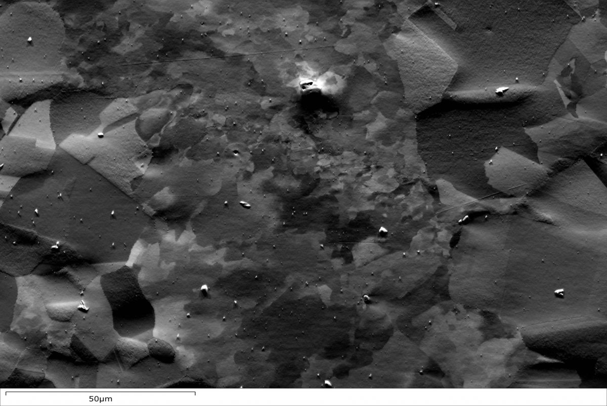
Forescatter orientation contrast electron image.
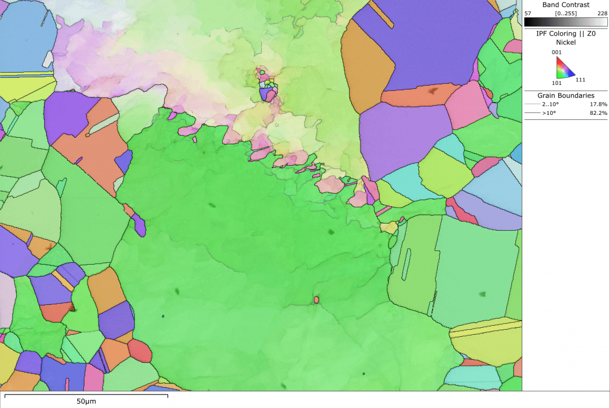
EBSD orientation map.
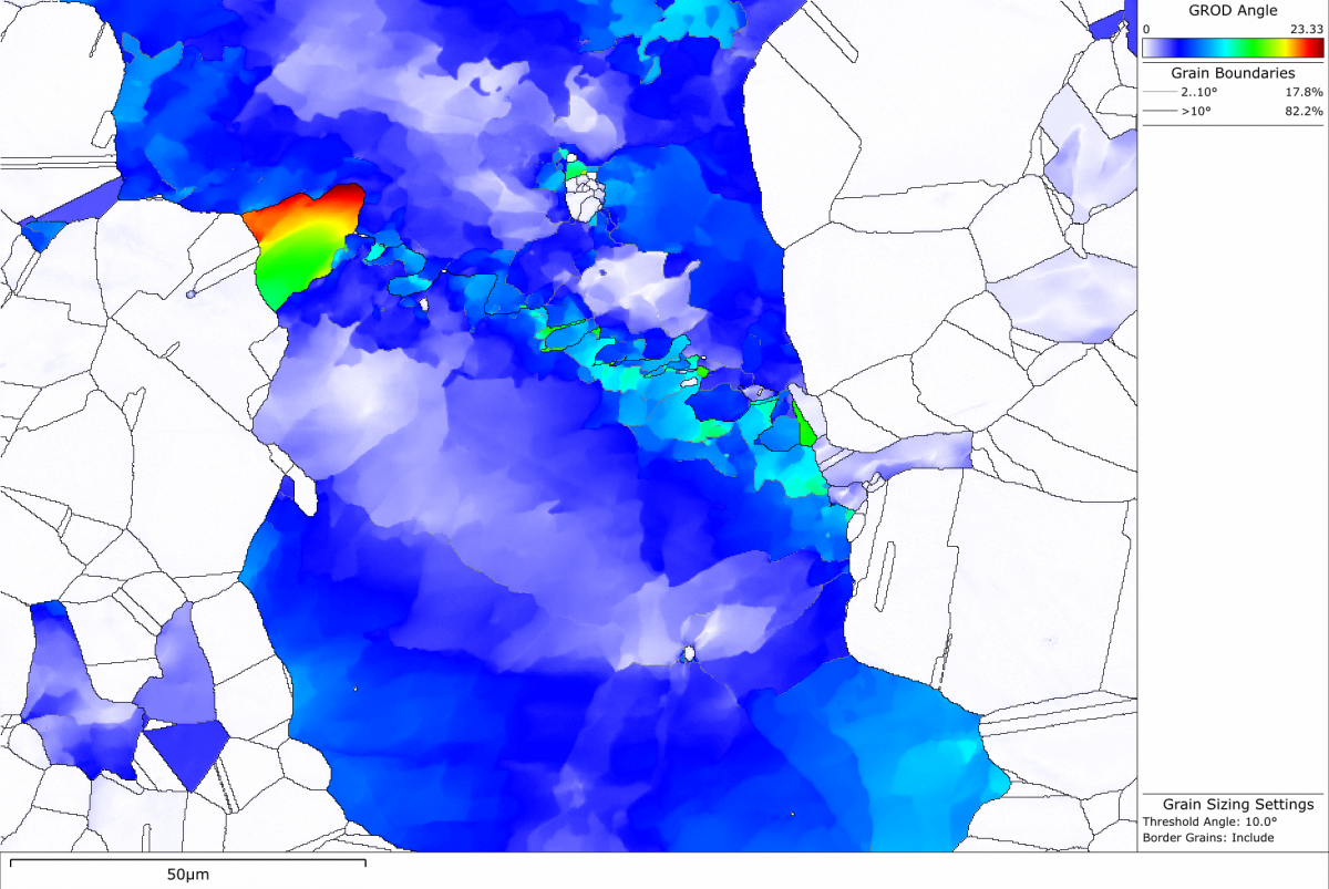
Grain relative orientation distribution angle map.
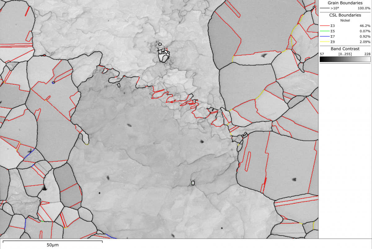
Pattern quality map with grain and coincident site lattice boundary overlay.
EBSD is unique in that it
provides a link between microstructure and crystallography. It complements
conventional analysis techniques by providing definitive information about the
crystal orientations present in the sample and, in combination with
compositional information using EDS, is the perfect tool for microstructural
characterisation.
© Oxford Instruments 2026