EBSD Explained
Techniques
Applications
Hints and Tips
Technology
OXFORD INSTRUMENTS EBSD PRODUCTS
CMOS Detector RangeAZtecHKL Acquisition SoftwareAZtecCrystal Processing Software
Electron Channelling Contrast Imaging (ECCI) is the most common name given to an imaging technique in the SEM that utilises the channelling effect of electrons with respect to crystallographic lattice planes. The contrast in the images is controlled by the crystallographic orientation of the lattice within each grain and can be used to give a rapid overview of the microstructure prior to Electron Backscatter Diffraction (EBSD) analyses.
If the crystal lattice is oriented suitably with respect to the electron beam, then ECCI images can be used to image and to characterise individual dislocations in the sample, thus providing information about slip systems and the mechanisms associated with deformation.
Although “ECCI” is a relatively new term, the use of backscattered electrons to image crystallographic contrasts in samples has been used for many decades. In the 1970s and 1980s, electron channelling patterns (ECPs) were used for the crystallographic analysis of materials science and geological samples in the SEM, with the same approach used for the collection of “channelling micrographs” (e.g Joy et al. (1982), Journal of Applied Physics 53, R81). As EBSD became an established technique in the 1990s, researchers started utilising backscattered electron (BSE) detectors mounted below the highly tilted samples required for EBSD analyses; these “forward scatter” or “forescatter” detectors also generated images based on the channelling of electrons in crystal lattice planes, giving rise to orientation contrast images.
The field of ECCI covers all of these approaches, but it is nowadays most commonly used with the sample in relatively low-tilt geometries, with the BSEs collected using pole-piece mounted detectors. In the tabs below, some of the key principles of ECCI are described along with some example application images.
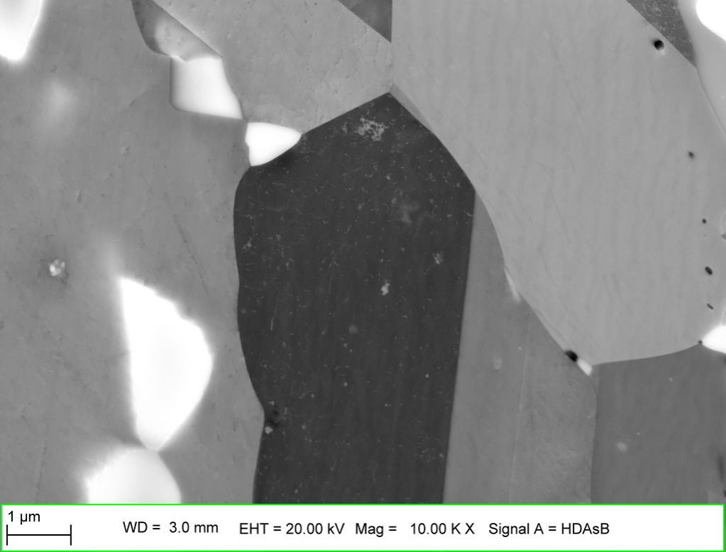
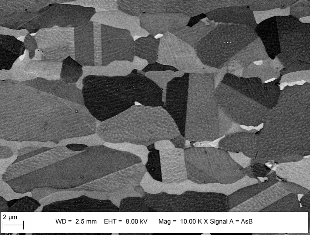
The main principle of ECCI involves the channelling of electrons down the lattice planes of crystalline materials. As the relationship between the incident electron beam and the crystal lattice orientations vary (e.g. between grains with different orientations), then the backscattered electron intensity will vary thus generating an image with different greyscale levels for different grains, as shown on the right.
This approach has been common for many years, and forms the basis of routine orientation contrast imaging using a standard pole-piece mounted BSE detector or forescatter detectors mounted below an EBSD detector’s phosphor screen.
However, if the sample is oriented so that, for a specific grain, the crystal lattice orientation satisfies the so-called two-beam diffraction condition, then any small change in the lattice orientation (such as caused by the presence of individual dislocations) will result in significant changes to the BSE intensity.
Therefore the dislocations will appear with a notable contrast change compared to their host grain.

ECCI image of a deformed and partially recrystallised Ni superalloy, collected using forescatter detectors in a high tilt geometry. Field of view ~300 mm across.

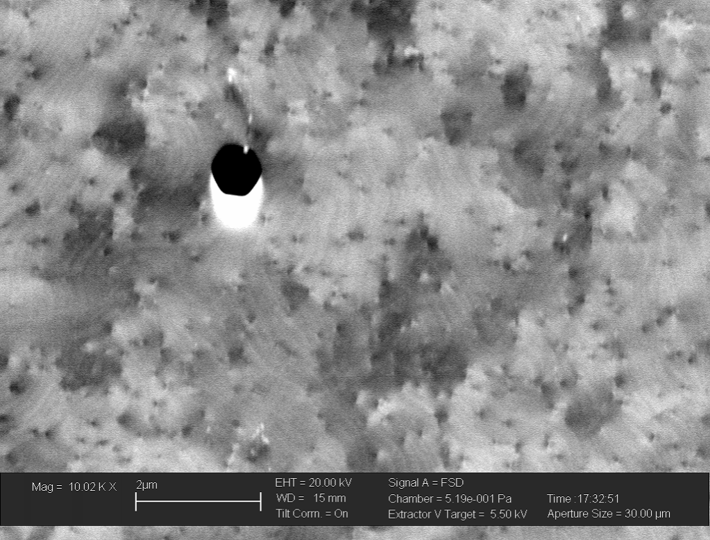
Example ECCI image of a dislocation network in UO2. Results and interpretations published in Mansour et al. (2018), Ceramics International, 45 (15), pp.18666-18671.
This approach is sometimes known as “controlled ECCI”, in that the orientation of the specific grain can be measured (for example, using prior EBSD or ECP orientation measurements) and then the ideal sample orientation calculated to obtain the two-beam diffraction condition.
In addition, knowing the orientation of the crystal lattice will enable determination of the type of dislocation that is being imaged. This controlled ECCI approach requires an accurate 5-axis stage and is often performed in the SEM using a dedicated motorised sub-stage.
ECCI is a very powerful technique, with the significant advantage over equivalent transmission electron microscope (TEM) approaches that it can be applied to bulk samples with just 1 free surface, and provides data from a much larger area of the sample. However, it can be time consuming to extract detailed dislocation characterisation, plus ECCI requires similarly high-quality surface preparation to that required for EBSD analyses. For some materials (especially those that oxidise readily, such as Mg or Al alloys), ECCI is not an effective technique


