
EBSD Explained
Techniques
Applications
Hints and Tips
Technology
OXFORD INSTRUMENTS EBSD PRODUCTS
CMOS Detector RangeAZtecHKL Acquisition SoftwareAZtecCrystal Processing Software
The spatial resolution of conventional Electron Backscatter Diffraction (EBSD) is inherently limited by the pattern source volume to effective resolutions in the order of 25-100 nm (the effective resolution takes into account the indexing routine’s ability to deconvolve overlapping EBSD patterns: the true resolution is significantly poorer). This is insufficient to accurately measure truly nanostructured materials (with mean grain sizes below 100 nm). The spatial resolution can be improved by reducing the beam energy (which in turn reduces the pattern source volume) and, with a suitably sensitive detector, it is then possible to characterise materials with sub-μm grain sizes. The orientation map to the right was collected from a fine-grained Ni sample using a beam energy of only 5 keV.
EBSD orientation map of a fine-grained Ni sample collected using a beam energy of 5 keV. The mean grain size in the fine-grained region is ~500 nm.

However, reducing the beam energy has other detrimental effects, including placing a higher demand on the sample preparation and making standard Hough-based indexing methods less effective (due to the broadening of Kikuchi bands in the EBSD pattern). An alternative approach is to use electron transparent samples coupled with a relatively high beam energy (e.g. 25-30 keV) and to image the diffracted electrons that have exited the lower surface of the sample. The interaction volume will be much smaller than when using conventional EBSD on a tilted bulk sample, as shown in the following Monte Carlo electron simulations.

Bulk sample tilted to 70° for conventional EBSD. Red regions correspond to electrons that have more than 93% of the incident beam energy.

Electron transparent sample (50 nm thickness). Red regions correspond to electrons that have more than 93% of the incident beam energy. The scales are the same for both images.
This new approach to SEM-based diffraction has been referred to as transmission EBSD (t-EBSD) but is more commonly referred to as transmission Kikuchi diffraction (TKD). The main reason to perform TKD analyses is to benefit from the improved spatial resolution, as this will enable effective characterisation of nanocrystalline materials and also of heavily deformed samples, where the high dislocation densities can prevent successful characterisation using conventional EBSD. Many studies have reported sub-10 nm resolution using TKD, although the sample atomic number, beam energy, sample thickness and tilt angle all influence the final spatial resolution.
TKD samples can be prepared with the standard methods used for transmission electron microscopy (TEM). For metals, electropolishing 3 mm diameter TEM discs is often the most effective as it can produce a large electron transparent region, but for non-conductive samples or when site-specific samples are required, preparation and sample lift-out using a focused ion beam scanning electron microscope (FIB-SEM) is highly effective. The optimum thickness will depend on the material, but for most samples 50-100 nm thickness is ideal.
For further information about the optimum thickness for TKD samples, refer to an application note on the subject here.
In the tabs below, you can explore more about the development of the TKD technique, including the different geometries that are commonly used, and some typical applications and example images.
There are 2 different geometries that are commonly used for TKD analyses: off-axis and on-axis. These are shown schematically in the following image.
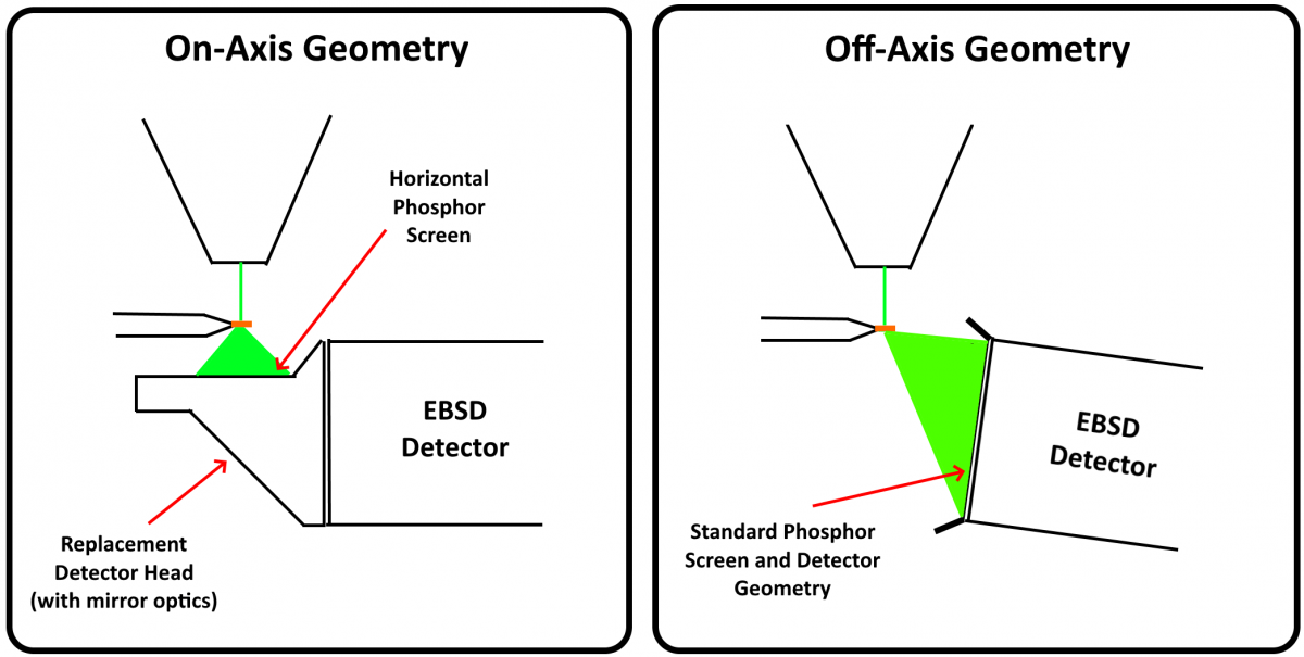
Schematic illustration showing on-axis and off-axis TKD geometries.
Both approaches have their respective benefits, but the performance and resolution are broadly similar. The table below compares the advantages and disadvantages of both TKD geometries.
| On-Axis TKD | Off-Axis TKD | |
| Hardware | Requires additional modified detector head | No extra hardware required |
| Ease of Switching from Standard EBSD | Detector head needs to be exchanged | Instantaneous |
| Sensitivity | Higher – captures more scattered electrons, but some signal loss due to mirror optics | Lower – electrons need to be scattered through higher angles |
| Distortion | None – pattern centred on phosphor screen | Significant – pattern centre at top edge of phosphor screen. Ideally requires an optimised band detection routine |
| Resolution | 2-10 nm | 2-10 nm |
| Darkfield Imaging | Yes – with various diode geometries | Yes – using lower forescatter diodes |
There are publications that have compared on and off axis geometries with regards to spatial resolution, and these indicate a minor benefit to using the on-axis approach. However, these used a backtilted (-20°) sample geometry for the off-axis case, which also has a significant detrimental impact on the spatial resolution, so the expected resolutions are broadly similar.
Note: details about Oxford Instrument’s optimised band detection routines developed for off-axis TKD can be found here.
You can read more about the historical development of TKD, plus a new sample preparation technique for off-axis TKD in some Oxford Instruments blog posts as follows:
TKD has been widely applied in a number of different applications, including on the following sample types:
The increased spatial resolution of the technique enables good quality diffraction patterns to be collected from materials that would be particularly challenging for regular EBSD. In the gallery below you can view some typical TKD maps from a range of different applications.

TKD phase map from a high pressure torsion deformed duplex steel. Field of view: 1 μm across

TKD orientation map from a high pressure torsion deformed duplex steel. Field of view 1 μm across
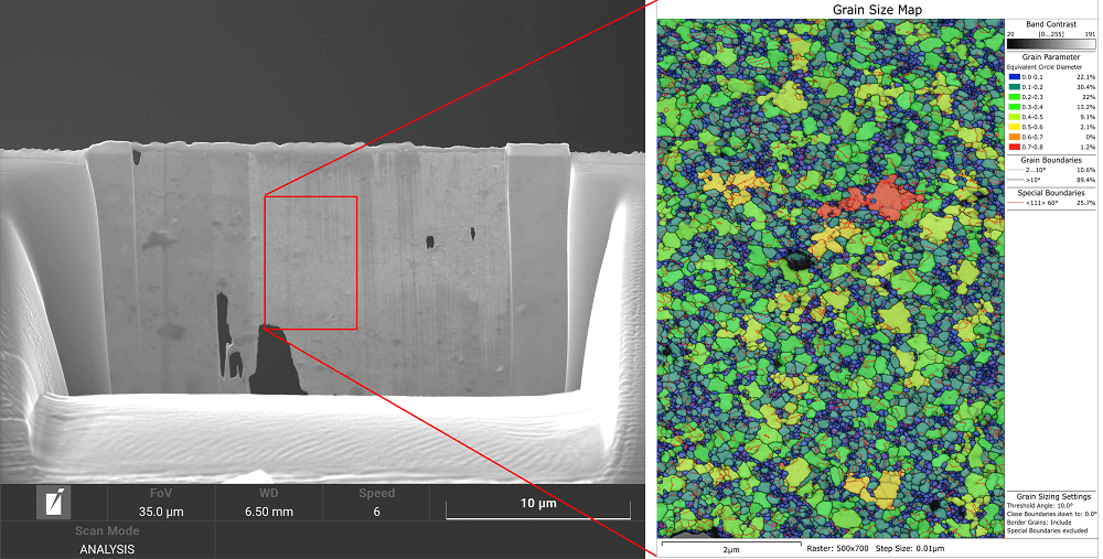
Secondary electron image (left) and subsequent TKD grain size map of a nanocrystalline Au thin film prepared using in-situ FIB milling. Map field of view: 5 μm across

Forescatter oriented darkfield image of a fatigued copper sample. Field of view: ~14 μm across.

Large area TKD orientation map of a martensitic steel. Retained Fe-FCC grains are coloured yellow. Field of view: 70 μm across.

TKD Phase map of a FIB lift out sample prepared from the edge of a chondrule in a carbonaceous chondritic meteorite. Field of view: 22 μm across. Sample courtesy of Luke Daly (University of Glasgow).
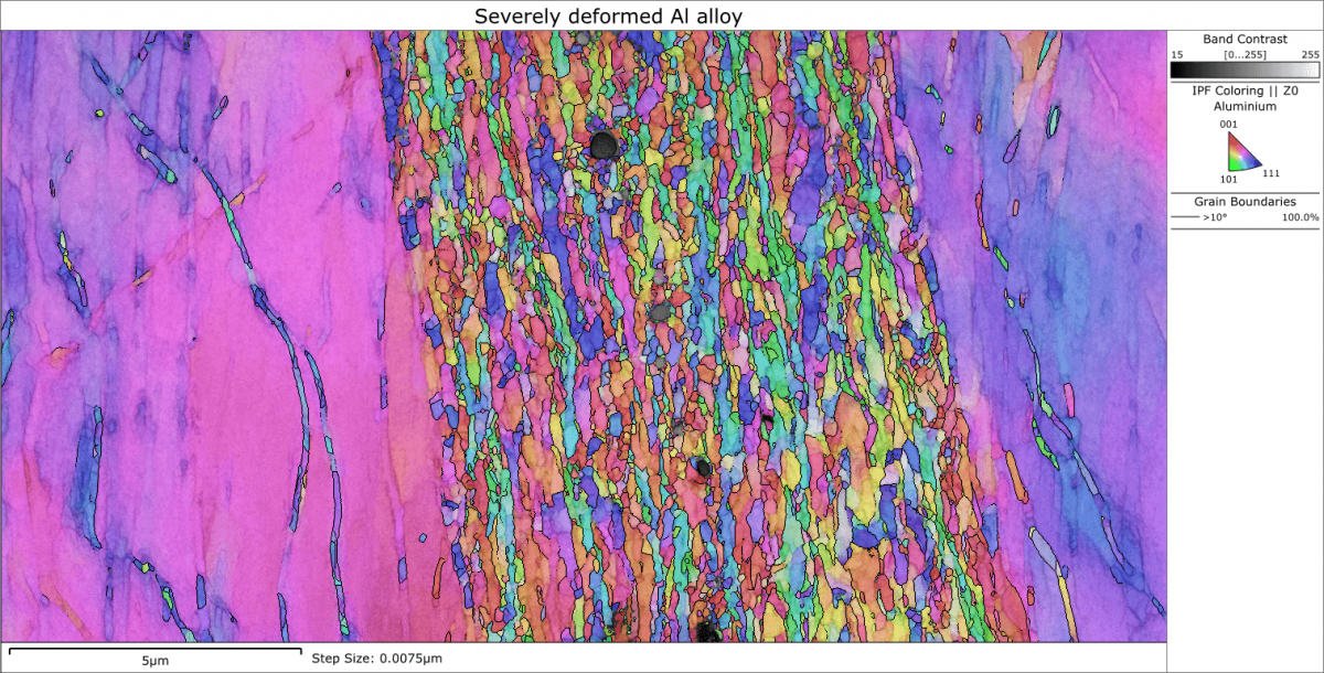
TKD orientation map of a nanocrystalline shear band in a deformed Al alloy. Field of view: 10 μm across.
© Oxford Instruments 2026